(1) ANGELS (Advanced Nanofab at GIST for Emerging Low-power Semiconductors)
- Purpose : To lead the paradigm shift in the semiconductor industry and secure the growth engine of regional industries by establishing AI semiconductor infrastructure and establishing AI semiconductor support base
- Service : (1) All fields of processes for AI semiconductors, (2) 3D integrated ultra-fine leading-edge processes, (3) Advanced back-end-of-line processes such as heterogeneous integration of chiplets and fan-out packaging, (4) Edge-Computing electronic and optical devices, (5) Gwangju-Jeonnam region-centered semiconductor industry-linked R&D, (6) Training field-based practical expert, corporate support, and R&D
- Construction period : 2023~2026 (4 years)
- Budget : Total KRW 39.05 billion (national budget KRW 26.65 billion / local budget KRW 12.4 billion)
- Use : 100/1000 class 6-inch process infrastructure
- Area : 5,520㎡ (Fab exclusive: 3,312㎡)


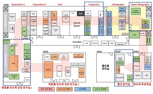
(2) G-NICS (GIST Nanoinfra for Compound Semiconductor)
- Use : 100/1000 class compound semiconductor process infrastructure
- Area : 400㎡
- Equipment : A total of 46 units
- Deposition: MBE, MOCVD, sputter, PECVD, ALD, evaporators
- Exposure: E-beam litho, hologram litho, photo litho
- Etching: RIE, ICP-RIE
- Back-end: CMP, lapping polishing, dicing machine
- Analysis: EL, PL, Raman, SEM, surface profiler, ellipsometer
- Milestones :
- 1996 Cleanroom completion
- 1997 Selected for the Excellent Research Center Support Program from the Korea Science and Engineering Foundation, through UFON (Ultrafast Fiber-Optic Networks) Research Center
- 2019 Follow-up process room expansion / GIST Central Research Equipment Center installation
- 2020 Selected for KIAT (Korea Institute for Advancement of Technology) Semiconductor Infrastructure Construction Support Project (Participation), Cleanroom Management Room Expansion
- 2021 Selected for NRF (National Research Foundation of Korea) University Nano Infrastructure Construction Support Project (Participation), Property Analysis Room Expansion
- 2022 Promoted to GIST Nanoinfra for Compound Semiconductor (G-NICS)
- 2023 Support for AI Semiconductor Advanced Process Fab Project

(3) GAIA (GIST Advanced Institute of Instrumental Analysis)
- Use : Material property analysis and component measurement infrastructure
- Area : 2,482㎡
- Equipment : A total of 59 units, including transmission electron microscopes with spherical aberration correction


